
White edges or white spots often appear during the routing processing of PCB, which will affect its performances. Jinzhou has concentrated on tools’ design and development for its whole life and has achieved great solution for the white problems. We are going to share the case with you as following.
Background:
Client A claimed that white edges generated at routing and forming courses while processing middle and high Tg boards, which needed to be solved urgently. The abnormality is as following:
![SKVE]LN[CVC365@$~J5QCKF.png](/upload/ueditor/image/20190225/6368668636032614816028373.png "SKVE]LN[CVC365@$~J5QCKF.png")
The analysis of the reason of the white problem:
When PCBs are affected by external mechanical force, especially when the external mechanical force of the boards is greater than the bonding force of the boards, the local resin of the boards will be separated from the glass fiber, thus forming white spots or white edges.
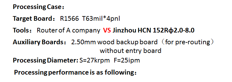
Jinzhou solution:

Conclusion:
During the processing of middle and high Tg boards, especially boards with high rigidity, brittle speciality and poor binding force, it is necessary to select routers with sharp cutting edges and good wear resistant property and apply appropriate diameters and processing parameters to reduce the external mechanical force.
Previous one:Jinzhou SHC Coating, No Worries
Address:Longgang High-tech Park, North longcheng Road, Longgang, Shenzhen, P.R.C
Phone:86-755-84877666
Fax:86-755-84878800
E-mail:sales@jinzhou.com.cn
jinzhou@jinzhou.com.cn

RichScan
Anti-fake check
CopyRight: SHENZHEN JINZHOU PRECISION TECHNOLOGY CORP. 粤ICP备12042779号-1
 中文
中文
 Shopping Cart
 Official Mall